


Market Overview
Semiconductor metrology instruments are designed for wafer and thin film in-line inspection after semiconductor processing. Semiconductor metrology instruments include ion manufactories, C- V systems, interferometers, source measure units (SME) magnetometers, optic and imaging systems, profilometers, reflectometers, resistance probes, and resistance high-energy electron diffraction (RHEED) systems, and X-ray diffractometers, among others.
According to Ken Research Analysis, the Global Semiconductor Metrology and Inspection Equipment Market is expected to record a positive CAGR of ~7% during the forecast period (2022-2028) and is expected to reach approximately US$ 15 billion by 2028.
 The global semiconductor metrology and inspection equipment market is driven by the rising demand for the miniaturization of electronic circuits in consumer electronic devices is driving the demand for the studied market. Additionally growing smart devices application, rising industrial automation, and widespread chip integration in vehicles propel the demand for semiconductors globally.
- Due to the increase in the number of smartphones and also due to the miniaturization of gadgets the proper inspection of the semiconductor manufacturing is important so that it does not cause any malfunction which results in a short circuit and damages the product.
The challenge faced by the global semiconductor metrology and inspection equipment market is the high dependence of countries like the USA on China for semiconductor parts. On the other hand, high investments and maintenance expenses and the complications of structure and functional defects in manufacturing procedures are expected to obstruct the market growth
- The USA’s dependent on China for semiconductor parts is a major challenge as the USA has imposed trade restrictions with China since 2018 and if this continues then the USA will suffer a major decrease in its market share. Furthermore, tariffs are applied in the import and export of goods which in turn increase the manufacturing price of the chips. Similarly, the recent conflict between China and Taiwan has also affected the trade of semiconductor parts globally.
COVID-19 heavily affected the global semiconductor metrology and inspection equipment market. Manufacturing sectors suffered severe losses due to factory shutdowns and fewer production volumes which prevented the growth of the automotive, electronics & semiconductor markets. In addition, there was a massive disruption in the supply chain across the region due to the lockdown measures, which further triggered a huge backlog of orders, and resulted in the loss of revenue for many large and small enterprises operating in the North American semiconductor metrology and inspection market.
Scope of the Report
The semiconductor metrology and inspection equipment market is segmented by type, and organization size. In addition, the report also covers market size and forecasts for the four major regions’ semiconductor metrology and inspection equipment market. The revenue used to size and forecast the market for each segment is US$ billion.
Key Trends by Market Segment
By Type: The lithography metrology type segment held the largest market share in the Global Semiconductor Metrology and Inspection Equipment Market in 2021.
- With nonstop transitions, such as the miniaturization of nodes and wafer sizes, the growth in demand for accelerating wafer sizes for ultra-large-scale integration fabrication technology has fostered the growth of lithography metrology equipment.
- In addition, a critical dimension scanning electron microscope (CD-SEM) is used for measuring the dimensions of the patterns formed on the wafer; the device is used as part of the manufacturing lines of electronic instruments and devices. Presently, CD-SEM has been witnessing significant demand, owing to the semiconductor output process.
 By Organization Size: The large enterprise segment held the largest share of the Global Semiconductor Metrology and Inspection Equipment Market in 2021.
- Large enterprises are generally the major end-user of the market. This comprises foundries, similar to TSMC and Global Foundry, and integrated device manufacturers, similar to Intel Corporation and Samsung which play a major part in the growth of this segment.
- In November 2021, Samsung Corporation declared to construct a semiconductor manufacturing unit in Texas due to the adding demand for chips for phones and other devices. The company planned to invest US$ 17 billion in constructing this unit. A significant part of that measure is anticipated to be employed for buying semiconductor metrology and inspection equipment. Similar strategic developments embraced by large enterprises are expected to drive the semiconductor metrology and inspection market growth for this segment.
By Geography: Asia Pacific accounted for the largest market share in 2021 within the total Global Semiconductor Metrology and Inspection Equipment Market.
- The Asia Pacific is one of the prominent regions for the semiconductor industry regarding manufacturing and application. According to the Secretariat of Industrial Approvals (SIA), Asia Pacific is the largest indigenous semiconductor market, and China is the largest single-country market.
- Additionally, in the region, the trend toward multiple-layer measurement is expanding due to the use of cluster deposition systems, where the lack of reality of single-layer measurement is driving the demand. Also, the fab manufacturers are shifting process monitors from bare wafers to production wafers due to the high cost and inspection challenges faced by the miniaturization of wafers.
Request For Sample Report @ https://www.kenresearch.com/sample report.php?Frmdetails=NTk2MTMx
 Competitive Landscape
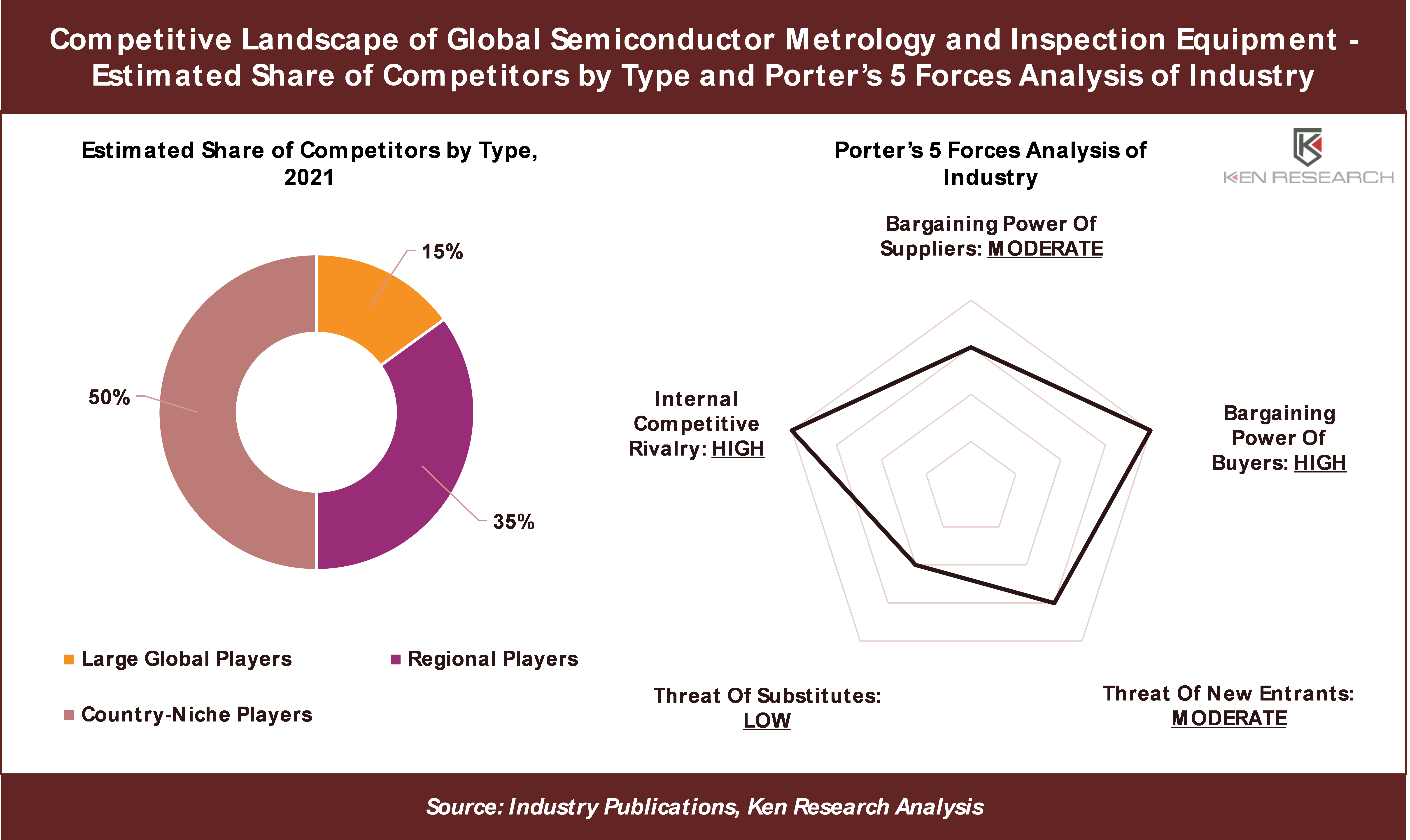
The global semiconductor metrology and inspection equipment market is highly competitive with ~150 players which include globally diversified players, regional players as well as a large number of country-niche players.
Country-Niche players comprise the highest share of 50% total competitors which is followed by the regional players holding a 35% share. Some of the major players in the market include KLA Corporation, Applied Materials Inc., Onto Innovation Inc. Thermo Fisher Scientific Inc., Hitachi High-Tech Corporation, Nova Ltd., ASML Holding NV, Lasertec Corporation., JEOL Ltd.., Nikon Metrology NV, Camtek Limited., Unity Semiconductor SAS, and others.
 Recent Developments Related to Major and Emerging Companies
- In July 2022, Onto Innovation Inc., declared the launch of its innovative acoustic metrology products. The new Echo system further expands the transferable request for in-line characterization of opaque films, which is estimated to be roughly USD 110 million, by using the principle of picosecond ultrasonic to deliver critical thickness metrology and material characterization for crucial technology transitions in the DRAM and high- stack NAND memory markets.
- In June 2022, Hitachi High-Tech Corporation declared the launch of the Hitachi Dark Field Wafer Defect Inspection System DI2800, a critical element in semiconductor manufacturers’ metrology capabilities. The DI2800 is a high-speed metrology system designed to identify faults and particles on patterned wafers up to 8 inches (200 mm) in diameter. Its high output and performance can help assure device trust ability and safety, particularly for largely sensitive operations like the Internet of Things (IoT) and automotive fields where 100 inspections are needed.
Key Topics Covered in the Report
- Snapshot of the Global Semiconductor Metrology and Inspection Equipment Market
- Industry Value Chain and Ecosystem Analysis
- Market size and Segmentation of the Global Semiconductor Metrology and Inspection Equipment Market
- Historic Growth of the Overall Global Semiconductor Metrology and Inspection Equipment Market and Segments
- Competition Scenario of the Market and Key Developments of Competitors
- Porter’s 5 Forces Analysis of the Global Semiconductor Metrology and Inspection Equipment Market
- Overview, Product Offerings, and SWOT Analysis of Key Competitors
- COVID-19 Impact on the Overall Global Semiconductor Metrology and Inspection Equipment Market
- Future Market Forecast and Growth Rates of the Total Global Semiconductor Metrology and Inspection Equipment Market and by Segments
- Market Size of Type / Organization Size Segments with Historical CAGR and Future Forecasts
- Analysis of the Semiconductor Metrology and Inspection Equipment Market in Major Regions
- Major Production / Consumption Hubs in the Major Regions
- Major Country-wise Historic and Future Market Growth Rates of the Total Market and Segments
- Overview of Notable Emerging Competitor Companies within Each Major Country
Request For Sample Report @ https://www.kenresearch.com/sample report.php?Frmdetails=NTk2MTMx
Major Players Mentioned in the report
- KLA Corporation
- Applied Materials Inc.
- Onto Innovation Inc.
- Thermo Fisher Scientific Inc.
- Hitachi High-Tech Corporation
- Nova Ltd.
- ASML Holding NV
- Lasertec Corporation
- JEOL Ltd.
- Nikon Metrology NV
- Camtek Limited
- Unity Semiconductor SAS
Notable Emerging Companies Mentioned in the Report
- Advantest Corporation
- Cadence Design Systems Inc.
- GCT Semiconductor Inc.
- Micross Silicon Turnkey Solutions
- INNOPHASE
Key Target Audience – Organizations and Entities Who Can Benefit by Subscribing This Report
- Metrology/Inspection Suppliers
- Semiconductor Processing Companies
- Semiconductor Manufacturers
- Wafer Fabrication Companies
- MOCVD Engineering Firms
- Semiconductor Research and Development Institutes
- Electronics Market Research & Consulting Firms
- Banking and Financial Institutions focused on Semiconductor Industry
- Semiconductor IP Suppliers
- Semiconductor Chip Manufacturers
- SoC and Hardware Suppliers
- Government & Regulatory Authorities
- PCB Designers and Manufacturers
- Components and Material Suppliers for Semiconductor Inspection Equipment
- Semiconductor Testing & Inspection Companies
- Government Ministries and Departments of Electronics Industry
Time Period Captured in the Report
- Historical Period: 2017-2021
- Forecast Period: 2022E-2028F
For more information on the research report, refer to below link:
Global Semiconductor Metrology Market
Follow Us
LinkedIn | Instagram | Facebook | Twitter | YouTube


