


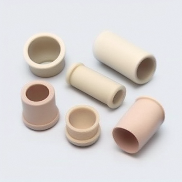
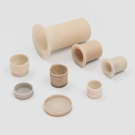
Aluminum nitride crucibles play a crucial role in the semiconductor manufacturing industry, particularly in the production of compound semiconductors. Compound semiconductors are materials composed of multiple elements and are used to create high-performance electronic and optoelectronic devices. Here's how aluminum nitride crucibles are applied in semiconductor manufacturing:
1. Epitaxial Growth: Epitaxy is a process used to grow a crystalline layer with a specific crystal structure on a semiconductor substrate. Aluminum nitride crucibles are employed to contain the source materials and facilitate the epitaxial growth of compound semiconductors.
2. Crystal Growth of GaN and SiC: Aluminum nitride crucibles are widely used in the process of crystal growth for gallium nitride (GaN) and silicon carbide (SiC) semiconductors. GaN and SiC are essential materials for high-power electronic and optoelectronic devices, such as LEDs, laser diodes, and high-frequency transistors.
3. Chemical Vapor Deposition (CVD): CVD processes utilize aluminum nitride crucibles to grow high-quality compound semiconductor layers on substrates. In CVD, chemical reactions occur at elevated temperatures, and the crucible plays a vital role in maintaining a stable and controlled environment.
4. MOCVD (Metal Organic Chemical Vapor Deposition): MOCVD is a specific type of CVD used for depositing thin semiconductor layers. Aluminum nitride crucibles are utilized to hold the metal organic precursors required for the MOCVD process.
5. Physical Vapor Deposition (PVD): Aluminum nitride crucibles are used in physical vapor deposition processes to deposit thin films of compound semiconductors on substrates. PVD is a common method for creating semiconductor layers with precise thickness and composition.
The choice of aluminum nitride crucibles in these semiconductor manufacturing processes is driven by the material's unique properties, such as high thermal conductivity, chemical stability, and resistance to high temperatures. These properties help ensure efficient heat transfer, uniform temperature distribution, and prevent contamination of the semiconductor materials during the growth process.


