


All silicon wafers are very beneficial for many functions. N-type silicon wafers utilized for advanced CMOS device production. Silicon wafers can be utilized for numerous reasons by their thickness and also flatness. Doped Silicon Wafer assists in the production of Si solar cells. Silicon wafers are produced by a thin slice of silicon that can be altered to make it work in several ways for different types of electric machines. Silicon wafers are semiconductors which used to manufacture integrated circuits and also integrated circuits in electronics.

Silicon is preferred over other semiconductors such as germanium for producing wafers due to its natural abundance and other features.
We all know that sand functions as a lightning conductor, but the same technique is used in computer and electronic circuit boards.One of Silicon's best features is that it can be combined with a wide range of other elements to create useful products, such as soap, shampoo, glass materials, medical implants, and enamel, as well as semiconductors.
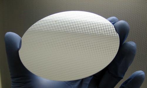
Chemically generated silicon cylinders, or ingots, are polished and cut into wafers of required thickness, then etched and polished again.The real technique for thin silicon wafer manufacturing is far more time-consuming and intricate, but the end product is a variety of wafers that may be utilized in a range of electronic devices.
Silicon wafers are produced from a single crystal of ultra-pure silicon, with impurities typically less than one part per billion.Integrated Circuits- A Common Application of Silicon WafersIntegrated Circuits An integrated circuit (IC), commonly known as a microchip or simply a chip, is a collection of electronic circuits embedded in a semiconducting substrate.
Although gallium arsenide is used in some applications, such as wireless communication devices, monocrystalline silicon is currently the most common substrate for ICs.
Wafers composed of silicon-germanium alloys are also becoming more popular, particularly in applications where the increased cost of silicon-germanium is justified.Most electrical gadgets now utilize integrated circuits (ICs), which have largely replaced discrete electronic components.

The global Silicon EPI Wafers Market research report, published by Value Market Research, is designed to offer various market framework such as market size, portion, trends, growth path, value and factors that impact the current market dynamics over the forecast period 2020-2027.
Most importantly, this report also provides the latest significant strategies adopted by major players along with their market share.The research report also covers the comprehensive profiles of the key players in the market and an in-depth view of the competitive landscape worldwide.
The major players in the silicon epi wafers market include Epiworks Inc., Global Wafers Japan Co. Pvt Ltd, Nichia Corporation, Siltronics AG, Silicon Valley Microelectronics Inc., Xiamen Powerway Advanced Material Co. Ltd, Visual Photonics Epitaxy Co. Ltd, Wafer Work, and American Elements.
This section consists of a holistic view of the competitive landscape that includes various strategic developments such as key mergers & acquisitions, future capacities, partnerships, financial overviews, collaborations, new product developments, new product launches, and other developments.Get more information on "Global Silicon EPI Wafers Market Research Report" by requesting FREE Sample Copy at https://www.valuemarketresearch.com/contact/silicon-epi-wafers-market/download-sampleMarket DynamicsIncreased adoption of this advanced wafer technology in electronics by consumers all over the world is the factor for triggering the demand for silicon epitaxial wafers and driving the market growth of silicon EPI wafers.
Rising demand for electronics such as laptops, tablets, and smartphones and the development of efficient and advanced technology are the major market drivers responsible for the market growth of silicon EPI wafers.
Owing to the high efficiency, lightweight, and less space consumption these are widely used in microprocessors and wearable technology.
