


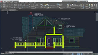
This AutoCAD Tutorial will explain how to set layers in AutoCAD in the electronics industry. While designing with AutoCAD, draft schemes. Burraq engineering solution provides AUTOCAD 2D 3D Training Course in Lahore. PCB masterpiece design, detailed catalogs, and assembly drawings are all drawn in different layers. Here is a description of the layers often created for the Electronic PCB design.
Silkscreen on the upper side of the PCB
The silkscreen contains a frame of parts and myths written in white ink on the upper side of the PCB. The manufacture of PCBs requires a mythical silk screen containing reference designers (parts).
The circuit traces the solder side of the PCB
Electronic schematics that include symbols representing the electronic components needed to create an AutoCAD drawing. These electronic symbols are connected to lines representing real electrical connections and are described in text containing details of the components used. Basic program features are scaled and available as a library to be used in AutoCAD which simplifies the process of producing schematics.
Pads in parts of the hole.
Endpoint sign libraries are available, with different types of holes and sizes, which need to be included in the diagram.
Patterns on the side of PCB components
Referee designers are used to specify the location of the components in the PCB, which are used during production, as well as to solve the PCB problem at a later date.
Grinding signs and features
The piercing properties of the drawings provide drilling details using the automatic drilling rigs.
Border drawing
A detailed list of components needed to make PCBs can be drawn from the AutoCAD diagram. Once the design is complete the AutoCAD drawing is converted to Gerber and Excellent file formats, which is the standard for the photo editing industry PCB artwork. These file formats are required for PCB manufacturing when using third-party add-on software.
· Research and educational institutions for the design of electrical systems.
· Electrical equipment companies for designing and manufacturing circuits, PCBs, and prototypes.
· Electrical engineers for designing and producing circuits, PCBs, and prototypes.
· Manufacturers extract information from drawings and use it for production.
AutoCAD Tutorial Summary
The use of these AutoCAD tutorials well as the libraries of the associated electronic components of electronic components, make the design and production of PCB structure easier.


Best institute for AutoCAD training in delhi is ducat.
Ducat provides best training in AutoCAD and also ducat provides live projects for all ducat students and also take 100% guaranty for placement and also ducat provides internship for all students.For more details please visit : Autocad coures in delhi

Chudasama Outsourcing Providing Structural BIM Services.BIM Software expertise Revit and AutoCAD.
Our structural BIM services include creating, generating construction documentation, BIM models extracting BIM components.

AutoCAD is the application that is used to design the model of machines or buildings which save these files in DWG format or Drawing file. If DWG files get corrupt then AutoCAD Recovery Tool can be used to repair .dwg files and restore data.
If these files get damaged then AutoCAD Recovery Tool repairs the corrupt .dwg files and recovers lost data with complete accuracy.
All objects like BLOCK, POINT, LINE, ARC, CIRCLE, ELLIPSE, SPLINE, XLINE, RAY, SOLID, 3DFACE, VERTEX & POLYLINE gets recover with same measurements ensuring Accuracy. It supports major AutoCAD vesrions and can be used with windows 10. Download AutoCAD Recovery Tool from http://www.filerepairtools.com/autocad-recovery-tool.html

The best AutoCAD Electronics software training is given by CADDSCHOOL.
CADDSCHOOL provides the AutoCAD classes it is based on electronics & communication field.
They are given field Related examples in Chennai.
CADDSCHOOL conduct the quality training & syllabus basis classes for AutoCAD Electronics design courses.http://www.caddschool.com/electronics-autocad-training-centre-in-chennai.php