


Printed Circuit Board (PCB) potting is a crucial process in the electronics industry, providing protection and enhancing the longevity of electronic components. This article delves into what PCB potting components are, their benefits, and the materials commonly used.
What is PCB Potting?
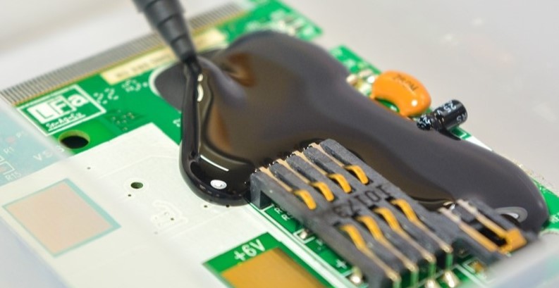
PCB potting involves encapsulating a printed circuit board with a solid or gelatinous compound. This protective layer shields the board and its components from environmental factors such as moisture, dust, and physical damage. Potting also improves the electrical insulation of the board, safeguarding it against short circuits and ensuring its reliable operation.
Benefits of PCB Potting
- Enhanced Durability: Potting significantly increases the mechanical strength of a PCB, making it more resistant to vibrations and shocks. This is especially important for applications in harsh environments, such as automotive or aerospace industries.
- Environmental Protection: The potting material acts as a barrier against environmental contaminants. It prevents moisture, dust, and chemicals from reaching the sensitive electronic components, thereby reducing the risk of corrosion and other forms of damage.
- Improved Insulation: By enveloping the PCB in an insulating material, potting reduces the likelihood of electrical shorts and improves overall circuit performance. This is crucial for high-voltage applications where electrical isolation is paramount.
- Thermal Management: Potting materials can help in dissipating heat generated by electronic components. This thermal management capability ensures that the PCB operates within safe temperature ranges, thus prolonging its lifespan and reliability.
Common Materials Used in PCB Potting
The choice of potting material depends on the specific requirements of the application. Some of the most commonly used materials include:
- Epoxy Resins: Known for their excellent mechanical strength and chemical resistance, epoxy resins are a popular choice for PCB potting. They provide robust protection and are suitable for use in harsh environments.
- Polyurethane Resins: These resins offer good flexibility and are ideal for applications where the PCB may be subjected to vibrations or mechanical stress. Polyurethane potting compounds also provide good moisture resistance.
- Silicone Compounds: Silicone potting materials are renowned for their flexibility and high-temperature resistance. They are often used in applications where thermal management is critical, as they can withstand extreme temperatures without degrading.
- Acrylic Compounds: Acrylics are used for their ease of application and removal. They offer good protection against moisture and are often chosen for applications where rework or repair of the PCB might be necessary.

Applications of PCB Potting
PCB potting is used across a wide range of industries and applications. Some common examples include:
- Automotive Electronics: In vehicles, PCBs are exposed to vibrations, heat, and environmental contaminants. Potting ensures these boards remain functional and reliable.
- Aerospace: Aircraft and spacecraft electronics require robust protection due to extreme operating conditions. Potting provides the necessary durability and insulation.
- Consumer Electronics: Devices such as smartphones, tablets, and wearables benefit from potting as it enhances their durability and water resistance.
- Industrial Equipment: Machinery and industrial control systems often operate in challenging environments. Potting helps protect their electronic components from dust, moisture, and mechanical damage.
Conclusion
PCB potting is an essential process that ensures the longevity and reliability of electronic components by providing protection against environmental factors and mechanical stresses. By choosing the right potting material, manufacturers can enhance the performance and durability of their products, making them suitable for a wide range of applications.
Understanding the benefits and materials involved in PCB potting is key to achieving optimal results in electronic device manufacturing.
Read more: https://www.pottingcompound.com


According to a new report published by Allied Market Research titled, "Potting Compounds Market by Resin Type, Curing Technique, Application, and End-user: Global Opportunity Analysis and Industry Forecast, 2014-2022", the potting compounds market was valued at $2,680 million in 2015 and is projected to reach $3,460 million by 2022, growing at a CAGR of 3.8% from 2016 to 2022.
The silicone resin type held nearly one-fourth of the total market in 2015.Potting compounds are used as a covering of the electronics and electrical devices to protect it from surrounding environment.
They offer protection from moisture and also provide heat dissipation, flame retardancy, and resistance from shock.
This is mainly attributed to their remarkable properties such as flexible protection against vibration, environmental contamination and thermal stress, excellent dielectric properties, and effective insulation against high voltages.Get Detailed COVID-19 Imapct Analysis for This Report: https://www.alliedmarketresearch.com/request-for-customization/1624?reqfor=covidElectronics and aerospace applications dominated the global potting compounds market with more than two-thirds share in terms of volume, in 2015.
Rise in transportation sector is the main reason for the growth of potting compounds market in the Asia-Pacific region.Read Report Overview: https://www.alliedmarketresearch.com/potting-compounds-marketThe major companies profiled in the report include Henkel AG & Co. KGaA, The 3M Company, MG Chemicals, ELANTAS GmbH, ALPAS srl, Dymax Corporation, Master Bond, Inc., Lord Corporation, Aremco Products, Inc., RBC Industries, Inc., and Shanghai Sepna Chemical Technology Co. Ltd.About Allied Market Research:Allied Market Research (AMR) is a full-service market research and business-consulting wing of Allied Analytics LLP based in Portland, Oregon.
Allied Market Research provides global enterprises as well as medium and small businesses with unmatched quality of "Market Research Reports" and "Business Intelligence Solutions."


Hydrocolloid dressing is a primary dressing that is used to treat uninfected wounds.
This dressing is easy to apply.