


Printed Circuit Board (PCB) potting is a critical process in the electronics industry, designed to protect electronic components and ensure their longevity. This article explores the concept of PCB potting components, their advantages, and the materials commonly used in this process. Get more here PCB potting compound.
What is PCB Potting?
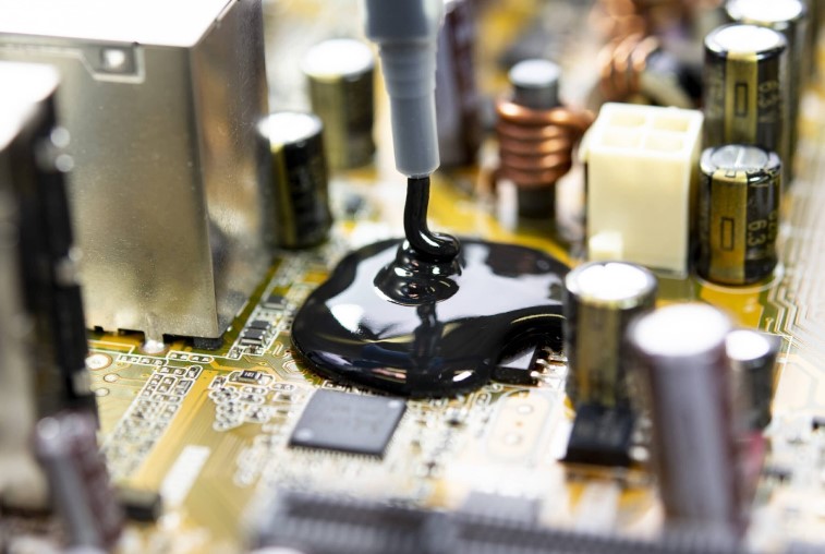
PCB potting is the process of encasing a printed circuit board with a protective material, which can be either solid or gel-like. This encapsulation shields the PCB and its components from environmental factors such as moisture, dust, and physical damage. Potting also enhances electrical insulation, reducing the risk of short circuits and improving the overall reliability of the PCB.
Advantages of PCB Potting
- Enhanced Durability: Potting significantly improves the mechanical strength of a PCB, making it more resistant to vibrations and shocks. This is particularly important for applications in demanding environments such as automotive or aerospace industries.
- Environmental Protection: The potting material forms a barrier against environmental contaminants, preventing moisture, dust, and chemicals from reaching the sensitive electronic components. This reduces the risk of corrosion and other forms of damage.
- Improved Insulation: Encasing the PCB in an insulating material reduces the likelihood of electrical shorts and enhances circuit performance. This is crucial for high-voltage applications where electrical isolation is essential.
- Thermal Management: Potting materials can help dissipate heat generated by electronic components. Effective thermal management ensures the PCB operates within safe temperature ranges, prolonging its lifespan and reliability.
Conclusion
PCB potting is an essential process that ensures the longevity and reliability of electronic components by providing protection against environmental factors and mechanical stresses.
By selecting the appropriate potting material, manufacturers can enhance the performance and durability of their products, making them suitable for a wide range of applications.
Understanding the benefits and materials involved in PCB potting is key to achieving optimal results in electronic device manufacturing.
Read more: www.pottingcompound.com


