


In the current hyper-connected world, wirelessly connecting is not an upscale feature; it is a promise. Compact connected devices are defining the future of the digital infrastructure, whether it is wearable health sensors and smart lighting systems, or digital industrial control nodes and smart logistics trackers. Nevertheless, the provision of dependable wireless communication in extremely small, battery-operated packages is among the greatest challenges to the engineering field. Product feasibility is determined by power consumption, cost, board space, certification, and integration complexity.
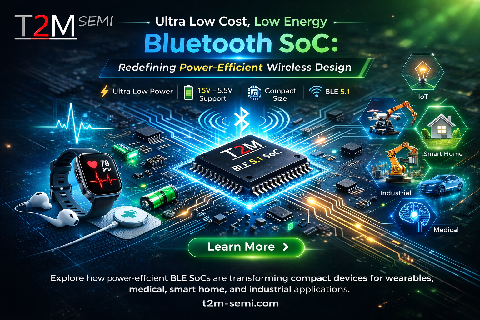
A Low Energy Bluetooth SoC An Ultra Low Cost Low Energy Bluetooth SoC specifically developed to fit compact battery-operated products, can overcome these limitations by incorporating wireless communication, processing, memory, power management, and peripheral interfaces in a single silicon solution. The SoC supports Bluetooth Low Energy (BLE) through version 5.1 and has advanced power optimization capabilities, allowing developers to create cost-efficient and power-saving products for the medical, consumer, industrial, and smart infrastructure sectors.
Designed for Extreme Power Efficiency
The fact that this SoC can be operated directly with a single 1.5 V battery cell is also one of the most striking qualities of this SoC. This saves a lot of complexity and costs of the system and avoids the multi-cell battery configurations that require large spaces. Long battery life can be more important than raw computational performance in the case of low-power systems like remote controls, wearable trackers, and RFID-based systems. The power management circuit has been incorporated in a way that ensures that it operates with a stable input voltage of 1.8V to 3.6V, but can also operate with a USB interface with a range of 4.5V to 5.5V.
Its embedded battery monitor will sense low-voltage situations and allow it to sense brownout conditions and come out of power-on-reset, providing stable and reliable operation. The concept of integrated LDO and DC-DC regulators also maximizes energy saving by ensuring the process of optimizing voltage regulation in various working modes.
The SoC uses around 5mA of power in the active mode at 3V. Current consumption in the sleep mode with SRAM retention reduces to approximately 1µA. Under external wake-up mode, power consumption may be lowered to 0.4 uA. These numbers allow it to be used in devices that have to run for months or even years using a small coin cell battery.
Compact Packaging for Space-Constrained Designs
The current IoT and wearable technologies require a small footprint. The SoC comes in a 1.6 × 2.0 × 0.5mm WLCSP and 3 × 3 × 0.55mm QFN24 package choices, which are extremely small. Other variants of the package, including TSOP16, offer the package to be flexible to the needs of various assemblies.
The chip-scale package WLCSP version is also highly desirable in very small designs like medical patches, smart rings and miniature sensor nodes. The device comprises five GPIO pins even in its smallest form whereas the QFN version has the capability of supporting up to twelve GPIOs to expand its functionality.
The bill-of-materials (BOM) savings made possible by this degree of integration, and the ease in PCB layout by this degree of packaging density. Embedded RF matching circuit and the possibility of operating inductively free allow further reduction of the number of external components and the total system cost by the designer.
High-Performance Wireless Connectivity
The SoC is Bluetooth Low Energy specification up to 5.1, which means compatibility with current Bluetooth Smart Ready phones, tablets, and medical devices. The improvements in BLE 5.x like the increase in throughput, the range and the coexistence capabilities enhance the reliability of the BLE in diverse environments.
Besides 1 Mbps and 2 Mbps, the transceiver can operate in Long Range mode and even in 250 kbps in IEEE 802.15.4. The support of not only ANT protocols, but also ANT+ protocols, also increases its capabilities in sports, fitness, and health ecosystems.
RF performance measures are competitive in the case of ultra-low-cost designs. The receiver sensitivity is -97 dormant -1 Mbps at BLE 1 Mbps and -100 dormant lemur to operate 802.15.4. The transmitter provides a maximum drive to +10 dBm, which makes it possible to use during long distances and ensure low-energy use.
This RF is what enables the SoC to be used in the smart home network, industrial sensor grid and smart transportation system where stable link quality is required.
Integrated Processing and Memory Architecture
The SoC has a proprietary microcontroller unit at the center with a processing unit and a 32-bit processor with up to 48 MHz speed. The MCU is power performance optimized as it has energy efficiency benefits over the traditional ARM implementation, Cortex-M0, within the same application segments.
The memory subsystem also has 64 kB Flash program memory and 32 kb of retention-capable SRAM. This layout is appropriately configured for the implementation of a BLE stack, application software, and peripheral management by the application of miniature devices in the IoT. The One-Time Programmable (OTP) memory is interna,l and it offers secure storage of configuration, making it flexible to configure production to any customization.
The solution provides reduced external dependencies as it incorporates processing, memory, and RF subsystems in one chip, enabling reduced firmware development of connected devices.
Robust Power Management Architecture
Energy-saving is the key component in the design of battery-operated products. The SoC has a variety of energy optimization mechanisms when active, idle, and in sleep. SRAM retention does not compromise state preservation because of fast wake-up. Other external wake-up options allow activation by an event, as would happen with sensors and human interface devices.
The DC-DC converter is integrated, so that it is higher in operating efficiency in the higher current mode, and the low-dropout regulator provides a constant supply in low-power mode. All these characteristics give a programmable power architecture capable of being used with multiple battery chemistries and models of use.
The fact that it has battery monitoring and brownout protection increases reliability, especially with medical and industrial setups where operation predictability is a requirement.
Digital and Analog Interface Flexibility
The SoC has a wide platform of digital and analog interfaces to accommodate a variety of system designs. The general-purpose input/output pins can be personally controlled with custom control, and the built-in 16-bit PWM can be used to control motors, dim LEDs, and generate waveforms.
There are communication interfaces such as the SPI, I2C, USB 2.0, and the UART. These interfaces allow the connection of sensors, displays, storage, and host processors without any difficulties. The USB 2.0 feature is of special use when the firmware needs updating, in diagnostics, or when a direct connection to a computer is needed.
Analog features are a 14-bit ADC and an in-built temperature sensor. These capabilities allow sensor-based applications like environmental scan, battery health scan, and wearable diagnostics without including any extra external ADC components.
Simplified RF Design and BOM Optimization
The RF front-end is one of the least considered product costs and design complexities. The SoC has an embedded matching circuit with RF, which is only slightly smaller in size than that of a standard RFID tag, which is why it does not require a massive matching network on the RFID card. Having fewer passive components and the ability to use no-inductor operation, designers are able to simplify layouts, as well as save on assembly expenses.
Timing can also be maximized by the use of an optional 32 kHz crystal. Depending on the needs of the applications, designers have the option of using external crystals because of the high accuracy or internal resources.
The integration can greatly reduce engineering work and shorten time to market, especially in cases where startups and OEMs are aiming at large consumer markets in high volumes.
Global Certification and Compliance
The wireless products venturing into foreign markets should be regulated by the regional standards. The SoC family has gained Europe certification of ETSI EN 300 328 and EN 300 440 Class 2 for Europe, the United States certification of FCC CFR47 Part 15, and the Japan certification of ARIB STD-T66.
The certifications make the process of product approval very easy and save time and cost incurred to carry out regulatory validation. The compliance of RoHS and the construction that was 100 percent lead-free also guaranteed compliance with the environment and the world standards in manufacturing.
Inbuilt compliance is significant to companies that are aiming at global implementation.
Broad Application Landscape
This SoC is packaged in ultra-low power consumption, small enclosure, high-performance RF, and combined with in-built peripherals, which will position the product in varied markets.
It is used in smartphones and tablet accessories to allow small Bluetooth devices like styluses, game controllers, and sound accessories. In the case of RF remote controls, it has a low sleep current, which makes their battery life very long even when used infrequently.
BLE and ANT are compatible with sports and fitness tracking devices, which allows them to be used in health ecosystems. The small size and low-power design of wearable devices and medical monitors are then used to create comfortable, lightweight products.
Its wireless features are used with smart lighting and smart home systems to create mesh networks and sensor-driven forms of automation. The 802.15.4 and the strong RF sensitivity provided by the SoC are powerful in building automation and smart grid applications to provide reliable communications over the distributed nodes.
Its ADC capabilities and temperature sensors are useful in industrial control and intelligent logistics systems to monitor the environmental conditions. The producers of consumer electronics value its affordability and reduced design demands.
Using its consistent connectivity and power efficiency, healthcare applications such as remote patient monitoring and portable diagnostic tools will be used to monitor solutions on a continuing basis.
Enabling the Next Wave of IoT Innovation
With the continuous growth of the IoT ecosystems, the performance, cost, and power consumption ratio become delicate. State-of-the-art silicon nodes can make the news; however, in practice, IoT deployment uses efficiency, reliability, and simplicity of integration.
A low-cost BLE SoC that brings wireless communication, MCU processing, memory, and power management and peripheral interfaces into a single compact device will enable developers to work on application innovation, as opposed to hardware intricacy.
Its capability to run on low battery sources, have ultra-low sleep currents, be able to support several wireless standards, and minimize external parts makes it a very useful base of scalable connected systems.
Conclusion
The Ultra Low-Cost Low-Energy Bluetooth SoC is a sensible and visionary approach to the wireless embedded design. It enables the development of essential IoT hardware through the integration of BLE 5.1 compatibility, multi-protocol RF support, compact packaging, built-in power management, and extensive digital interfaces, which address the key concerns of IoT hardware development.
In the case of manufacturers of medical devices, wearable electronics, smart infrastructure, industrial monitoring, and consumer accessories, this SoC provides cost-effectiveness, power savings, and consistency of performance.
The next generation of wireless innovation will center around this type of integrated SoC platform as smaller, smarter, and energy-conscious connected devices are integrated and designed.


